


 LinkedIn
 Meta Muse AI Agent Lands on Apple Watch and Wear OS
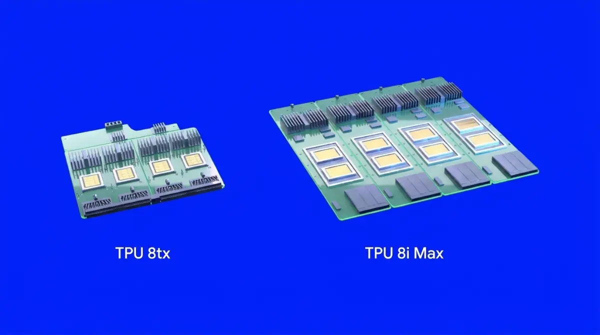
Google Unveils TPU 8tx and TPU 8i Max AI Processors
Google expanded its eighth-generation Tensor Processing Unit lineup with two specialized chips, introducing the encrypted TPU 8tx for confidential computing and the high-memory TPU 8i Max for massive context windows, while bringing TPUs to Oracle Cloud.
Umar Abubakar | · 7 min read

Deploying a single, monolithic computer chip to handle every artificial intelligence task has become an expensive engineering mistake. In the early gold rush of machine learning, cloud providers bought general-purpose graphics processors in bulk, using the identical silicon dies to train massive foundation models, serve lightweight chatbot prompts, and parse sensitive enterprise databases. That one-size-fits-all hardware strategy created operational waste: server clusters burned excessive electrical power running simple inferences, while regulated enterprises avoided cloud deployments because processor memory lacked hardware-grade encryption. Alphabet cloud division moved to dismantle that silicon compromise on Tuesday, November 10, 2026. The search giant announced the expansion of its eighth-generation custom silicon portfolio, unveiling two specialized processor architectures: the TPU 8tx, built for encrypted confidential computing, and the TPU 8i Max, engineered for massive context window inference. Concurrently, Google announced a historic commercial alliance with Oracle Cloud Infrastructure to host TPU clusters in Oracle data centers starting in 2027, marking the first time Google proprietary processors will be available outside Google Cloud. The chip launches arrive as server developers diversify hardware stacks, continuing semiconductor developments we followed when Amazon made its Trainium custom processors compatible with PyTorch.
The product announcements mark an important architectural shift inside Google Systems Infrastructure group. Historically, Google maintained a predictable hardware release rhythm: designing and manufacturing a single major Tensor Processing Unit generation every two years. The arrival of TPU 8tx and TPU 8i Max indicates that Google has abandoned that rigid cadence in favor of specialized workload targeting. Instead of forcing enterprise customers to pay for unused compute features, Google is spinning off tailored variants built on its proven eighth-generation architecture. The TPU 8tx pairs Google tensor silicon with custom security processors and AMD EPYC server CPUs to keep corporate data encrypted in memory during active processing, cutting data exposure risks for commercial banking and healthcare clients. The TPU 8i Max attacks the memory capacity wall: packaging expanded High-Bandwidth Memory pools to serve models processing millions of tokens simultaneously. By pairing hardware specialization with third-party cloud distribution through Oracle, Google is positioning its TPU portfolio as a direct commercial alternative to Nvidia dominant accelerator lineup. Silicon design buyouts and hardware packaging match trends we documented when Marvell acquired Lumentum in a $115B optical deal.
TPU 8tx: Hardware Confidentiality for Regulated Enterprises
To inspect why the TPU 8tx matters to enterprise buyers, one must examine the security vulnerabilities of modern server clusters. In standard cloud computing, customer data is encrypted when stored on solid-state drives and encrypted when transmitted across fiber optic networks.
The moment an algorithm processes data, the information must be decrypted inside processor memory registers. If a malicious insider, a hostile nation-state hacker, or a compromised hypervisor breaches the host server, raw customer records sitting in memory can be stolen. Regulated organizations: including commercial investment banks, defense contractors, and hospital systems: refuse to run sensitive data through public cloud models due to this memory exposure risk. The TPU 8tx solves this vulnerability through hardware-level Confidential Computing. Developed in partnership with AMD, the TPU 8tx isolates model execution inside cryptographically sealed memory enclaves using AMD Secure Encrypted Virtualization (SEV-SNP). Data remains encrypted while flowing across processor interconnects and inside High-Bandwidth Memory dies, decrypting only inside arithmetic logic units. Google confirmed that the TPU 8tx delivers twice the processing speed of previous confidential cloud instances with zero performance degradation, allowing banks to audit fraud and hospitals to parse patient genomes without exposing raw data to cloud administrators. Hardware security perimeters and cryptographic defenses match systems we analyzed when Anthropic developed FlashProve to verify model identity.
TPU 8i Max: Conquering the Multi-Million Token Context Wall
While the TPU 8tx targets corporate security, the TPU 8i Max addresses the computational bottlenecks created by long-context reasoning models. When an application queries a model with two million tokens of background text: such as a complete legal case archive or an entire operating system codebase: the attention mechanism requires immense memory bandwidth.
In standard accelerator clusters, serving long-context prompts requires distributing the query across dozens of server cards, introducing networking latency as processors exchange attention key-value caches over copper cables. The TPU 8i Max re-engineers the memory hierarchy: mounting ninety-six gigabytes of ultra-dense HBM3E memory dies directly onto the processor substrate with an expanded memory bus. The chip features an enlarged on-die SRAM scratchpad that holds intermediate attention weights locally, reducing trips to external memory by forty percent. In practical enterprise benchmarks, the TPU 8i Max processes multi-million-token queries three times faster than standard eighth-generation chips while lowering electrical power consumption per query by twenty-eight percent. Software developers building autonomous coding assistants, mathematical theorem provers, and biochemical drug discovery pipelines can feed complex technical datasets into model contexts without experiencing memory throttling. Memory component supply constraints were detailed in our report on SK Hynix discussing memory chip plant agreements.
Comparing Cloud Hyperscaler Custom AI Silicon
| Processor Hardware | Developer Organization | Primary Architectural Focus | Memory Packaging Spec | Cloud Availability Channel |
|---|---|---|---|---|
| Google TPU 8tx | Google (Alphabet) | Encrypted confidential enterprise AI | 64GB HBM3E (Hardware encrypted) | Google Cloud & Oracle OCI (2027) |
| Google TPU 8i Max | Google (Alphabet) | Long-context inference & memory bandwidth | 96GB high-density HBM3E | Google Cloud & Oracle OCI (2027) |
| AWS Trainium3 | Amazon Annapurna Labs | Ultra-low-cost foundation training | 96GB HBM3E memory | Locked exclusively to AWS Bedrock |
| Microsoft Maia 300 | Microsoft Silicon Group | Azure OpenAI Copilot workloads | 64GB HBM2E packaging | Locked exclusively to Azure internal |
| Nvidia B200 (Blackwell) | Nvidia Corporation | Universal high-density training & inference | 192GB HBM3E dual-die substrate | Merchant market across all cloud hosts |
The comparative data illustrates how Google is challenging Nvidia merchant market monopoly. While Amazon Trainium and Microsoft Maia chips remain locked behind their own proprietary cloud platforms, Google is breaking out of its walled garden. Partnering with Oracle Cloud Infrastructure allows Google to sell TPU computing time to enterprises that already run database operations on Oracle servers, expanding its silicon market share. While Nvidia B200 commands gross profit margins near eighty percent, Google custom TPUs cost significantly less to fabricate at TSMC, allowing Google and Oracle to price computing instances at aggressive discounts. Cloud server procurement agreements were explored in our analysis of HPE securing server contracts with cloud providers.
The Oracle Partnership: Breaching Cloud Isolation
The decision to bring Google TPUs onto Oracle Cloud Infrastructure marks an important commercial truce between two longtime software rivals. For two decades, Google and Oracle engaged in fierce legal and commercial battles, fighting all the way to the Supreme Court over Java programming code.
In the high-stakes computational era, operational pragmatism has replaced ancient corporate feuds. Oracle Chief Executive Officer Safra Catz built OCI into an infrastructure destination by signing long-term hosting deals with artificial intelligence leaders like OpenAI and Cohere. Oracle lacked a competitive in-house custom processor, relying entirely on expensive Nvidia chips. By welcoming Google TPUs into Oracle facilities, Oracle offers customers an alternative accelerator that lowers operating costs. For Google, the deal transforms its TPU hardware division from an internal cost center into an enterprise silicon business. Google captures hardware licensing fees and software runtime revenues on every TPU cycle executed inside Oracle facilities, without spending Google capital to build new physical buildings. Corporate alliances across software leaders match strategies we followed when Nvidia invested $3B in Meta to secure hardware ties.
The Road Forward for Specialized Silicon Architectures
Google introduction of the TPU 8tx and TPU 8i Max delivers a definitive verdict on the trajectory of semiconductor hardware: the era of general-purpose computing processors is drawing to a close. As machine reasoning models expand into specialized industrial sectors, hardware must adapt to the physical contours of the workload.
By engineering specialized silicon for encrypted corporate data and massive context windows, Google proved that thoughtful architectural adaptation beats raw transistor counts. Distributing those chips through Oracle Cloud breaks the traditional cloud walled gardens, creating a more competitive, diverse semiconductor marketplace. As enterprises deploy the TPU 8tx and TPU 8i Max in early 2027, the technology industry will benefit from having reliable, affordable hardware alternatives. In the ongoing computational century, true leadership will not belong to the chipmaker that builds the biggest processor, but to the disciplined architects who craft the precise tools needed to solve the real, practical challenges of the modern world.
Read More on TechRobust:
Umar Abubakar
Umar Abubakar
Expertise:Editorial Leadership, Product Design (UI/UX), Digital Media Strategy, Technology Systems, Product Architecture
Award:TechRobust Visionary Leader of the Year 2025
Umar serves as Editor-In-Chief of TechRobust, combining editorial vision with senior product design expertise to shape how modern technology stories are built, packaged, and told. Overseeing all editorial verticals, he directs coverage across global and regional tech industry while applying deep design thinking to publication strategy and reader experience.
Related Stories
Meta Muse AI Agent Lands on Apple Watch and Wear OS Trump Signals Openness to Guardrails in Race With China
 Decision Models Like Jev Won't Explain Their Answers